PCB Manufacturing Process.
The technology industry is constantly evolving and the future for PCBs is growing coincidently with it.

Printed Circuit Board – An Overview

Printed circuit board (PCB) is a highly reliable and durable physical circuit design that has become an essential component of any electronic device. Printed circuit boards are made of a very thin substrate board embedded with electronic components interconnected using thin-layer of copper interconnecting traces. The board substrate is usually made of fiberglass composite epoxy substrate or other laminate materials. The circuit will contain both active and passive components. With more advanced and smaller component availability it is possible to accommodate a very large and complex circuit in a small PCB design.

PCBs are of three types. Single side, Double side, and Multi-layered boards. Single-sided boards have the components on one side of the substrate. Double side have components on both sides. In a multi-layered board, multiple layers of printed circuits are separated by insulation layers. In double-sided and multilayer PCBs components are interconnected by drilling holes at appropriate points and plating them with conducting materials.

Major Advantages of PCB

1.Smaller and Thinner in size.

2.Highly customizable in design and application.


3.Durable, Reliable and long life.


4.Easy to debug and easy to repair.


5.Low cost.

Various Steps in PCB Design and Manufacturing


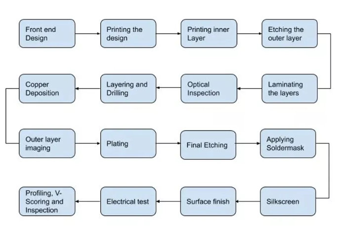
Step 1: Requirement analysis and Component selection

The first step in PCB design is to analyze the requirement and select the appropriate components such as processor, power supply. Create a blueprint that fulfills all the requirements

Step 2: In-System Front end design
PCB layout is initially designed using a PCB design software. Altium Designer, Autodesk EAGLE, KiCad EDA, OrCAD are some commercially available software used for PCB design. The output of this design is usually in the form of a PCB schematic Gerber file. Gerber file encodes information including copper tracking layers, drill drawing, component notation, and other parameters.

Step 3: Photo tool Initiation

Next step is to run Design for Manufacture (DFM) check before circuit boards fabrication starts. This is to avoid any discrepancies in design. After this, a photo film is made to image the PCB using a laser printer/plotter. Different layers of the PCB photo film are aligned by punching precise registration holes in each sheet of film. The film is created to help in creating a figure of copper path.


Step 4: Printing the inner layers
The substrate, usually a composite epoxy substrate is taken, cut, cleaned and dried. Copper is pre-bonded on both sides of the substrate. Cleanliness of the panel is the most important factor to avoid short or open circuit errors. The copper is coated with a layer of photoresist, which then treated with UV light to harden it. The film formed in the previous step is placed over the copper layer and aligned using pin positions.

Later the panel is again UV treated. The dark areas on the film do not allow UV light, thus the areas below dark areas of the film are not hardened. While the light areas that are meant for copper wiring are hardened.

Step 5: Etching out the unwanted copper
The panel is then washed with an alkaline solution to wash away unhardened copper material. The desired copper layer is fully protected beneath the hardened layer of photoresist.

Next, the photoresist that is over the copper layer is also removed. This, in turn, leaves only the required copper layer intact.

Step 6: Register punching for layer alignment
The different layers are aligned and optically punched to create registration holes. This will align the inner layers to the outer layers.

Step7: Automated optical inspection
After lamination, it is impossible to sort out errors in inner layers. Hence the panel is subjected to automatic optical inspection before bonding up and lamination. The machine scans the layers using a laser sensor and compares it with the original Gerber file to list out discrepancies, if any.

Step 8: Layer up and Bond 
The layers of the PCB panel are bonded together by aluminium press plate. For double and multi later PCB further copper foils are pressed over original layers with insulating layers placed in between and the etching process is repeated. Finally, all the layers are laminated together to provide the final shape to the PCB panel.

Step 9: Drilling
The PCB stack is then drilled for holes. These holes are where the electronic components of the PCB including via holes are to be placed and interconnected. Holes are drilled with a diameter of approximately 100 to 150 microns. Precision is the key to the drilling process. Laser locator or X-Y coordinate systems are used to achieve precision.

Step 10: Copper Deposition and Platting
This step is to cover the entire panel with a fresh layer of copper after drilling. It bonds the panels and also covers the nonconductive materials opened up after drilling. A chemical electrolysis setup is used for plating. The drill holes are covered with around 25 microns of copper to ensure proper connection.

Step 11: Outer layer imaging and copper etching
Similar to step 3 a photoresist material is applied over the outer copper layer and then they are imaged. Tin guard covering is provided over the required copper area as a protection and the other unwanted copper is removed. PCB connections are established after this step.

Step 12:  Solder Mask Application
The board is now cleaned and the solder mask is applied. Solder mask is to protect the board from copper oxidation, damage, and corrosion. An Epoxy is applied along with a solder mask which gives the usual green color to the board. Unwanted solder mask is removed by exposure to UV light. Then the board is oven-baked.

Step 13: Gold or Silver surface finish
The PCB is then plated with gold, silver or lead-free HASL or hot air solder leveling finish. This is done so that the components are able to be soldered to the pads created and to protect the copper.

Step14:Silkscreen
The silk-screening or profiling is the process of printing all of the critical information on the PCB, such as manufacturer id, company name component numbers, debugging points. This stands useful while service and repair.

Step 15: Electrical test
Electrical test is done using probe testers. Open and short circuit tests are performed. Electrical tests ensure functional reliability. Durability testing are also performed after functional test.

Step 16: V-Scoring
The actual PCB is cut out from the manufactured panel. PCB is cut out in specific sizes and shapes based upon the customer design and as per the original Gerber file date.

V-cuts are made along the sides of the board which permits the board to easily pop out from the panel.

Step 17: Final inspection and packing

PCB is subjected to final visual inspection and quality inspection. Test reports are provided for customer verification. Vacuum sealed or airbag/air pocket packaging is done to prevent any physical damage to the boards.


Conclusion

PCB design process is a requirement driven and highly customizable process enables us to produce specific circuit function whether complex or simple. Cleanliness and precision are the most important precautions to be followed in PCB design and manufacturing


Limelight IT Research Private Limited, Tarun Purohit 4 April, 2022
Share this post
Tags
Archive
Industry Demanding Software’s for Engineering Freshers
With growing economy, India is witnessing the growth of education sector. However, Indian industry is not so convinced about the job-readiness of the graduates.